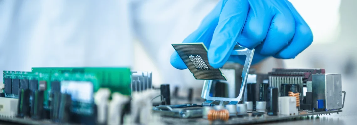
Semiconductor repair services play a crucial role in the electronics industry, offering a lifeline for costly and complex integrated circuits. As chips become increasingly sophisticated and miniaturized, the need for specialized repair techniques has never been more critical. From nanoscale defect detection to advanced packaging repair, these services employ cutting-edge technologies to diagnose and fix issues that could otherwise lead to significant financial losses and production delays.
The semiconductor industry relies heavily on precision and reliability. When a chip fails or malfunctions, it can have far-reaching consequences, affecting everything from consumer electronics to industrial machinery. This is where expert repair services step in, utilizing a range of advanced techniques and tools to breathe new life into damaged or faulty semiconductors.
Semiconductor failure analysis techniques for precision repair
Failure analysis is the cornerstone of effective semiconductor repair. By accurately identifying the root cause of a chip’s malfunction, repair technicians can develop targeted solutions that address the specific issue at hand.
Scanning electron microscopy (SEM) for nanoscale defect detection
Scanning Electron Microscopy (SEM) is an indispensable tool in the semiconductor repair toolkit. This powerful imaging technique allows technicians to visualize defects at the nanoscale level, providing unprecedented insight into the physical structure of a chip. By bombarding the sample with a focused beam of electrons, SEM creates high-resolution images that can reveal even the tiniest imperfections.
SEM is particularly useful for detecting issues such as:
- Microscopic cracks in chip substrates
- Contamination particles on chip surfaces
- Defects in metal interconnects
- Irregularities in transistor structures
The ability to identify these nanoscale defects is crucial for developing precise repair strategies and ensuring the long-term reliability of repaired semiconductors.
Focused ion beam (FIB) circuit edit and microsurgery
Focused Ion Beam (FIB) technology represents a quantum leap in semiconductor repair capabilities. This technique allows technicians to perform intricate microsurgery on integrated circuits, modifying or repairing specific components without damaging surrounding structures. FIB systems use a beam of ions (typically gallium) to mill away or deposit material with nanometer-scale precision.
Some key applications of FIB in semiconductor repair include:
- Cutting and rewiring metal interconnects
- Depositing conductive or insulating materials to fix open or short circuits
- Creating cross-sections for internal inspection
- Repairing mask defects in chip production
The precision offered by FIB technology enables repairs that would be impossible with conventional methods, often saving chips that would otherwise be discarded.
Time-domain reflectometry (TDR) for signal integrity assessment
Time-Domain Reflectometry (TDR) is a powerful diagnostic tool used to assess signal integrity in high-speed circuits. This technique involves sending a fast-rise-time pulse down a transmission line and analyzing the reflections that occur due to impedance discontinuities. In semiconductor repair, TDR helps identify issues such as:
- Broken or damaged traces on printed circuit boards
- Impedance mismatches in high-frequency signal paths
- Faulty connectors or solder joints
- Degradation in transmission line quality
By pinpointing these signal integrity issues, repair technicians can focus their efforts on the specific areas that require attention, improving the overall performance and reliability of the repaired semiconductor device.
Thermal imaging for hotspot identification in ICs
Thermal imaging is an invaluable technique for identifying hotspots and thermal anomalies in integrated circuits. Using specialized infrared cameras, technicians can create heat maps of operating chips, revealing areas of excessive power consumption or potential failure points. This non-invasive method is particularly useful for:
- Detecting short circuits that cause localized heating
- Identifying components operating outside their thermal specifications
- Assessing the effectiveness of heat dissipation solutions
- Locating areas of high current leakage
By addressing these thermal issues, repair services can significantly extend the lifespan and improve the reliability of repaired semiconductors.
Advanced chip packaging repair methodologies
As semiconductor packaging becomes more complex, with technologies like 3D integration and advanced interconnects, repair methodologies must evolve to meet these challenges. Modern chip packaging repair requires a combination of precision techniques and specialized equipment to address issues without compromising the integrity of the delicate internal structures.
Ball grid array (BGA) rework and reballing procedures
Ball Grid Array (BGA) packages are ubiquitous in modern electronics, offering high pin counts in a compact form factor. However, their complexity makes repair challenging. BGA rework and reballing procedures involve carefully removing the chip from the board, replacing damaged solder balls, and precisely realigning the component.
Key steps in BGA repair include:
- Preheating the board to reduce thermal stress
- Removing the faulty BGA component using specialized hot air tools
- Cleaning and preparing the board pads
- Applying new solder balls using a reballing stencil
- Precisely aligning and reflowing the repaired BGA
These procedures require a high level of skill and specialized equipment to ensure proper alignment and reliable connections. At eumetrys-robotics.com , advanced robotic systems are employed to achieve the precision required for successful BGA repairs.
Flip chip underfill removal and reapplication
Flip chip technology, where the semiconductor die is directly connected to the substrate via solder bumps, presents unique challenges in repair scenarios. The underfill material, which provides mechanical strength and thermal protection, must be carefully removed and reapplied during the repair process.
The flip chip repair process typically involves:
- Softening the underfill using targeted heat application
- Mechanical removal of the softened underfill
- Cleaning and preparing the substrate and die surfaces
- Precise reapplication of new underfill material
- Curing the underfill to restore mechanical integrity
This delicate procedure requires a deep understanding of materials science and precision application techniques to ensure the repaired flip chip maintains its reliability and performance characteristics.
Through-silicon via (TSV) repair in 3D-ICs
Through-Silicon Vias (TSVs) are a critical enabling technology for 3D-integrated circuits, allowing for vertical interconnections between stacked dies. Repairing TSVs presents significant challenges due to their embedded nature and the risk of damaging surrounding structures.
Advanced TSV repair techniques may include:
- Laser-assisted via reveal for accessing buried TSVs
- Focused Ion Beam (FIB) for precise material removal and deposition
- Conductive material refilling using advanced deposition techniques
- Non-destructive testing to verify repair integrity
These sophisticated repair methodologies require state-of-the-art equipment and highly skilled technicians to successfully restore functionality to complex 3D-IC structures.
ESD and latch-up protection strategies for sensitive components
Electrostatic Discharge (ESD) and latch-up events can cause catastrophic failure in semiconductor devices. Implementing robust protection strategies is essential for ensuring the longevity and reliability of repaired chips. Expert semiconductor repair services employ a multi-faceted approach to ESD and latch-up protection.
Key protection strategies include:
- Implementing on-chip ESD protection structures
- Designing robust power distribution networks to mitigate latch-up risks
- Utilizing advanced ESD-safe handling procedures during repair processes
- Incorporating guard rings and substrate taps to prevent parasitic bipolar action
By integrating these protection measures into the repair process, technicians can significantly reduce the risk of ESD and latch-up related failures in repaired semiconductor devices.
Cleanroom protocols for Contamination-Free semiconductor repair
Maintaining a contamination-free environment is paramount in semiconductor repair. Even microscopic particles can cause catastrophic failures in highly integrated circuits. State-of-the-art repair facilities adhere to stringent cleanroom protocols to ensure the highest levels of cleanliness and precision.
Essential cleanroom practices include:
- Utilizing HEPA and ULPA filtration systems to remove airborne particles
- Implementing strict gowning procedures for technicians
- Employing laminar airflow systems to minimize particle movement
- Regular monitoring and certification of cleanroom environments
These protocols are not just guidelines but critical components of the repair process, ensuring that repaired semiconductors meet the same stringent quality standards as newly manufactured chips.
Specialized tools and equipment for High-Precision chip repair
The complexity of modern semiconductors demands an array of specialized tools and equipment for effective repair. These advanced instruments enable technicians to perform intricate operations with nanometer-scale precision, ensuring the highest quality repairs.
Plasma cleaning systems for surface preparation
Plasma cleaning systems play a crucial role in preparing semiconductor surfaces for repair. By using ionized gases, these systems can remove organic contaminants and oxides at the molecular level, creating an ultra-clean surface for subsequent repair processes.
Benefits of plasma cleaning in semiconductor repair include:
- Enhanced adhesion for underfills and encapsulants
- Improved bond strength in wire bonding processes
- Reduction of contact resistance in electrical connections
- Removal of stubborn flux residues and other contaminants
The use of plasma cleaning technology ensures that repaired semiconductors maintain optimal electrical and mechanical properties.
Ultrasonic wire bonders for interconnect restoration
Ultrasonic wire bonders are indispensable tools for restoring or modifying chip interconnections. These precision instruments use a combination of ultrasonic energy and pressure to create solid-state bonds between fine wires and chip pads or leadframes.
Key capabilities of advanced wire bonders include:
- Automated pattern recognition for precise bond placement
- Multi-axis control for complex bonding geometries
- Real-time bond quality monitoring and adjustment
- Compatibility with a wide range of wire materials and diameters
The precision offered by these wire bonders allows for the repair of even the most intricate chip packages, restoring functionality to damaged or modified semiconductors.
Automated optical inspection (AOI) for quality assurance
Automated Optical Inspection (AOI) systems are crucial for ensuring the quality and reliability of repaired semiconductors. These systems use high-resolution cameras and advanced image processing algorithms to detect defects that may be invisible to the human eye.
AOI systems in semiconductor repair can identify:
- Misaligned or missing components
- Solder joint defects
- Surface contamination
- Damaged or incorrect markings
By integrating AOI into the repair workflow, technicians can verify the quality of their work and catch potential issues before they lead to field failures.
Laser decapsulation systems for package access
Laser decapsulation systems provide a non-destructive method for accessing the internal components of packaged semiconductors. By precisely removing encapsulation material, these systems allow technicians to perform repairs or modifications without damaging the delicate chip structures beneath.
Advantages of laser decapsulation include:
- Selective removal of package material
- Minimal thermal and mechanical stress on the chip
- Ability to create precise openings for probing or repair
- Compatibility with a wide range of package types and materials
This technology enables repairs that would be impossible with traditional mechanical decapsulation methods, expanding the range of semiconductors that can be successfully repaired.
Data recovery techniques for damaged memory chips
When memory chips suffer physical damage or electrical failure, critical data can be at risk. Advanced semiconductor repair services employ specialized techniques to recover data from damaged memory devices, often providing a last resort for retrieving irreplaceable information.
Data recovery techniques for damaged memory chips may include:
- Direct probing of memory cells using nano-probers
- Chip-off techniques to access raw NAND or NOR flash memory
- Custom firmware development for bypassing damaged controller chips
- Laser-assisted chip deprocessing for accessing internal memory structures
These advanced recovery methods require a deep understanding of memory architectures and specialized equipment to successfully retrieve data from severely damaged chips.