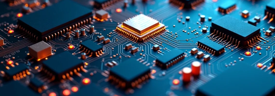
Double sided printed circuit boards (PCBs) have become an indispensable component in modern electronics design. These versatile boards offer significant advantages over their single-sided counterparts, enabling engineers to create more compact, efficient, and high-performance electronic devices. By utilizing conductive layers on both sides of the substrate, double sided PCBs provide enhanced functionality and design flexibility that is crucial in today’s fast-paced technological landscape.
The benefits of double sided PCBs extend far beyond simple space-saving measures. From improved signal integrity to superior thermal management, these boards empower designers to overcome many of the challenges associated with complex circuit design. As electronic devices continue to shrink in size while simultaneously increasing in functionality, the role of double sided PCBs in meeting these demanding requirements becomes ever more critical.
Enhanced signal integrity in double sided PCB designs
One of the most significant advantages of double sided PCBs is their ability to enhance signal integrity. In electronic circuits, maintaining clean and reliable signals is paramount for ensuring optimal performance and reducing errors. Double sided PCBs offer several features that contribute to improved signal integrity:
- Shorter trace lengths
- Better control over impedance
- Reduced electromagnetic interference (EMI)
- Improved ground plane distribution
By allowing components to be placed on both sides of the board, designers can significantly reduce the distance between interconnected elements. This reduction in trace length directly translates to lower signal propagation delays and decreased parasitic inductance, both of which are critical factors in maintaining signal quality.
Furthermore, the ability to use ground planes on both sides of the board provides better shielding against electromagnetic interference. This shielding effect is particularly important in high-frequency applications where signal integrity can be easily compromised by external noise sources.
Thermal management advantages of dual layer PCBs
Effective thermal management is a critical consideration in electronic design, particularly as devices become more powerful and compact. Double sided PCBs, available on icape-group.com, offer significant advantages in this area, providing designers with more options for managing heat dissipation and maintaining optimal operating temperatures.
Heat dissipation through copper pour techniques
One of the most effective thermal management techniques available in double sided PCB design is the use of copper pour. This method involves filling large areas of unused board space with copper, which serves as an excellent heat conductor. By implementing copper pour on both sides of the board, designers can create a more efficient heat dissipation system.
Copper pour areas can be strategically placed near heat-generating components, providing a direct path for thermal energy to spread across the board. This technique is particularly effective when combined with thermal vias, which allow heat to transfer between the top and bottom layers of the PCB.
Thermal vias implementation for temperature control
Thermal vias are small, plated through-holes that provide a low-resistance path for heat to travel between PCB layers. In double sided designs, these vias can be used to create a highly effective thermal management system. By placing thermal vias around heat-generating components and connecting them to copper pour areas on both sides of the board, designers can significantly improve heat dissipation.
Proper implementation of thermal vias can lead to temperature reductions of up to 30% in some designs, making them an invaluable tool in managing the thermal characteristics of electronic devices.
Balanced component distribution for optimal cooling
Double sided PCBs allow for a more balanced distribution of components, which can have a significant impact on thermal management. By spreading heat-generating components across both sides of the board, designers can avoid creating concentrated hot spots that are difficult to cool.
This balanced approach to component placement allows for more efficient use of cooling techniques such as heat sinks and forced air cooling. It also helps to ensure that no single area of the board becomes excessively hot, which can lead to reduced performance or even component failure.
Electromagnetic interference (EMI) reduction in double sided PCBs
Electromagnetic interference is a pervasive challenge in electronic design, capable of causing signal degradation, data errors, and even system failures. Double sided PCBs offer several advantages in mitigating EMI, making them an excellent choice for designs where electromagnetic compatibility is a critical concern.
Ground plane shielding strategies
One of the most effective EMI reduction techniques available in double sided PCB design is the use of comprehensive ground planes. By dedicating one layer (or significant portions of both layers) to a continuous ground plane, designers can create an effective shield against electromagnetic radiation.
Ground planes serve multiple purposes in EMI reduction:
- They provide a low-impedance return path for currents
- They act as a barrier to electromagnetic fields
- They help maintain consistent reference voltages across the board
The ability to implement extensive ground planes on both sides of a double sided PCB significantly enhances its EMI shielding capabilities compared to single-sided designs.
Differential pair routing for EMI mitigation
Differential pair routing is another powerful technique for reducing EMI in double sided PCB designs. This method involves routing two complementary signals in close proximity to each other, typically on opposite sides of the board. The electromagnetic fields generated by these signals tend to cancel each other out, resulting in reduced overall EMI.
Double sided PCBs are particularly well-suited for differential pair routing, as they allow for precise control over trace length and spacing. This level of control is crucial for maintaining the signal integrity of high-speed differential pairs, such as those used in USB or HDMI interfaces.
Split power planes to minimize crosstalk
In addition to ground planes, double sided PCBs allow for the implementation of split power planes. This technique involves dividing the power distribution system into separate regions, each dedicated to supplying power to specific circuit sections.
Split power planes offer several benefits in terms of EMI reduction:
- They help isolate noise-sensitive circuits from noise-generating ones
- They reduce the coupling of noise between different power domains
- They allow for more precise control of power distribution
By carefully designing split power planes on a double sided PCB, engineers can significantly reduce crosstalk and improve overall electromagnetic compatibility.
Space optimization and component density in dual layer boards
One of the most compelling advantages of double sided PCBs is their ability to dramatically increase component density while optimizing space utilization. This characteristic is becoming increasingly crucial as electronic devices continue to shrink in size while simultaneously expanding in functionality.
Double sided PCBs allow designers to place components on both sides of the board, effectively doubling the available surface area for component mounting. This increased real estate translates directly into higher component density, enabling the creation of more complex circuits within a smaller form factor.
Space optimization in double sided PCBs goes beyond simple component placement. These boards also allow for more efficient routing of traces, often resulting in designs that require fewer vias and shorter overall trace lengths. This efficiency not only saves space but also contributes to improved signal integrity and reduced electromagnetic interference.
The ability to achieve higher component density with double sided PCBs has far-reaching implications for electronic product design. It enables the creation of smaller, more portable devices without sacrificing functionality. This is particularly important in industries such as wearable technology, mobile devices, and IoT (Internet of Things) applications, where size and weight are critical factors.
Double sided PCBs can increase component density by up to 50% compared to single-sided designs, while maintaining or even improving overall performance.
Cost-effectiveness of double sided PCBs vs. multilayer alternatives
While multilayer PCBs offer even greater design flexibility and component density than double sided boards, they also come with significantly higher costs and longer production times. For many applications, double sided PCBs strike an optimal balance between performance and cost-effectiveness.
The cost advantages of double sided PCBs over multilayer alternatives stem from several factors:
- Simpler manufacturing process
- Lower material costs
- Shorter production times
- Reduced complexity in design and testing
These factors combine to make double sided PCBs an attractive option for a wide range of applications, particularly in medium-volume production runs or prototyping scenarios where the additional complexity of multilayer boards may not be justified.
It’s important to note that the cost-effectiveness of double sided PCBs doesn’t come at the expense of performance. For many designs, especially those that don’t require the extreme component density or signal isolation capabilities of multilayer boards, double sided PCBs can provide all the necessary functionality at a fraction of the cost.
Design flexibility and prototyping ease with Two-Layer PCBs
Double sided PCBs offer significant advantages in terms of design flexibility and ease of prototyping. These characteristics make them an ideal choice for rapid product development and iterative design processes.
Through-hole and surface mount technology (SMT) integration
One of the key advantages of double sided PCBs is their ability to seamlessly integrate both through-hole and surface mount components. This flexibility allows designers to choose the most appropriate component type for each function without being constrained by board limitations.
Through-hole components, which are inserted through holes in the board and soldered on the opposite side, offer excellent mechanical strength and are often preferred for high-reliability applications. Surface mount components, on the other hand, are smaller and can be placed at higher densities, making them ideal for compact designs.
The ability to use both types of components on a single board gives designers the freedom to optimize their designs for performance, cost, and manufacturability.
Via-in-pad design for complex routing solutions
Via-in-pad design is a technique that involves placing vias directly within component pads, rather than adjacent to them. This approach offers several advantages in terms of routing flexibility and space optimization.
Double sided PCBs are particularly well-suited for via-in-pad designs, as they allow for efficient use of both board surfaces. This technique can significantly reduce the overall footprint of a design, enabling higher component densities and more compact layouts.
Via-in-pad technology is especially beneficial for BGA (Ball Grid Array) components, where space for routing between pads is extremely limited. By incorporating vias directly into the pads, designers can create more efficient routing schemes and improve overall signal integrity.
Impedance control techniques in double sided layouts
Impedance control is crucial for maintaining signal integrity in high-speed digital designs. Double sided PCBs offer several techniques for achieving precise impedance control, including:
- Microstrip line configurations
- Stripline configurations (when used with ground planes)
- Coplanar waveguide structures
These techniques allow designers to maintain consistent impedance along signal paths, reducing reflections and ensuring clean signal transmission. The ability to implement these impedance control methods on both sides of the board provides greater flexibility in routing and component placement.
Mixed-signal circuit separation strategies
In designs that incorporate both analog and digital circuits, maintaining proper separation between these different signal types is crucial for preventing interference and ensuring optimal performance. Double sided PCBs offer effective strategies for achieving this separation.
One common approach is to dedicate one side of the board to analog circuits and the other to digital circuits. This physical separation, combined with proper ground plane design, can significantly reduce the risk of digital noise coupling into sensitive analog signal paths.
Additionally, the ability to implement split planes on double sided PCBs allows for further isolation between different circuit sections. This technique can be particularly effective in mixed-signal designs where multiple power domains are required.
The flexibility offered by double sided PCBs in terms of circuit separation makes them an excellent choice for prototyping mixed-signal designs. Engineers can quickly iterate on their layouts, experimenting with different separation strategies to achieve optimal performance.